- 글번호
- 1136039
Konkuk University-Korea University research team implements the world's first silicon-based integrated continuous wave nano laser at room temperature
- 작성자
- 관리자
- 조회수
- 2332
- 등록일
- 2024.09.26
- 수정일
- 2024.09.27
- The article has been published in 'Science Advances', a world-renowned academic journal.
- Breakthrough in Silicon Optical Integrated Circuit Technology

△From left, Professor Noh Yoo-shin (Corresponding author, Konkuk University), Professor Kim Myung-ki (Corresponding author, Korea University), Park Byung-joon (first author, Korea University), Kim Min-woo (first author, Konkuk University)
Professor Noh Yoo-shin (Department of Physics) of Konkuk University succeeded in realizing the world's first silicon-based integrated continuous wave nanolaser at room temperature with a research team from Korea University's KU-KIST Graduate School of Converging Science & Techonlogy. The results were published on Sept. 19, 2024 in Science Advances, a world-renowned journal and sister journal of Science.
This achievement overcomes important technical limitations in the development of next-generation Photonic Integrated Circuits (PICs) and is an ultra-precise integration of silicon nanolasers capable of continuous wave operation at room temperature. This technology is attracting attention as a key element of next-generation optical communication systems.
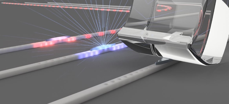
Silicon, which is used as a core material for electronic and optical integrated circuits, cannot emit light by itself, so developing a light source in silicon-based optical integrated circuits has long had technical difficulties. To solve this problem, a method of combining a light-generating III-V semiconductor with silicon has been attempted and with some success, but implementing continuous wave oscillation at a nanoscale remained a big challenge due to thermal instability and inefficient light focusing problems. In particular, nanometer-sized lasers are prone to excessive absorption and scattering losses due to their small volume, which often caused problems such as suppression of oscillation or a sharp increase in laser thresholds.
△ A schematic diagram of the 'on-demand minimal-gain printing' technique for precisely implanting nanometer-sized light emitting materials into silicon optical integrated circuits
In order to solve this technical difficulty, this study introduced a new concept 'on-demand minimal-gain printing' technique that precisely inserts a minimum of III-V semiconductor material into a silicon nano resonator. This technique is designed so that the laser amplification takes place inside the silicon circuit after implanting only the light-emitting gain material required for laser oscillation to a minimum, rather than implanting the existing completed laser into a silicon-integrated circuit.
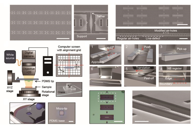
△ Process of producing silicon nanolasers at room temperature continuously through the 'On-demand minimal-gain printing' technique
Through this, it was possible to achieve significantly higher thermal stability and lower oscillation thresholds compared to conventional nanolasers while minimizing the use of expensive III-V materials. As a result, it succeeded in implementing an integrated continuous wave silicon nanolaser that operates at a low power of 50 µW or less at room temperature. This technology can be easily integrated into silicon wafers without a complicated manufacturing process, which is expected to greatly accelerate the commercialization of silicon photonics and optical integrated circuits.
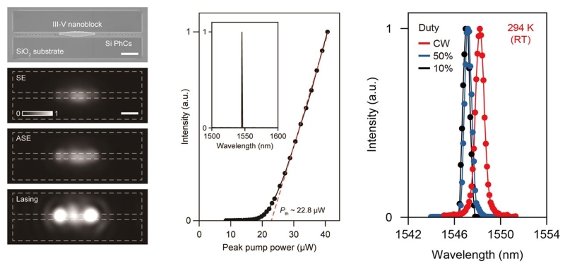
△Electron scanning microscope image of nanolaser device, light emission characteristics (left) of nanolaser, laser operation based on pumping power, and laser oscillation spectrum results under room temperature (RT) continuous wave (CW) pumping conditions (right)
Professor Noh Yoo-shin (Department of Physics) of Konkuk University emphasized, "This study has made an important breakthrough in the completion of silicon optical integrated circuit technology and will serve as an opportunity to greatly increase the commercial implementation possibility of silicon optical integrated circuits." Professor Kim Myung-ki of Korea University's Graduate School of Convergence at KU-KIST added, "This technology is a key element of next-generation optical communication and high-performance optical integrated circuits and can be widely applied to various types of integrated devices as well as lasers."
The study was conducted with the support of the Korea Research Foundation's mid-sized researcher support project.